What Is the Valence Band in a Semiconductor?
Learn the difference between valence and conduction bands, what a band gap is, and how electrons carry current in semiconductors.
What Is the Valence Band in a Semiconductor?
SCIENCE EXPLAINED • US ENGLISH • EDITORIAL SNAPSHOT: NOVEMBER 1, 2026
The valence band is a range of allowed electron energies in a solid that is filled, or nearly filled, under appropriate low-energy conditions. The conduction band is a higher-energy range in which electrons can move through a material and contribute to electrical conduction. Their separation—the band gap—is central to understanding semiconductors, LEDs, solar cells, and many electronic devices.
Why electron energies form bands
In an isolated atom, electrons occupy discrete energy levels. In a crystal containing enormous numbers of atoms, interactions between neighboring atoms create closely spaced allowed energies that physicists group into bands. Some energy ranges between the bands are forbidden for ordinary electronic states in the ideal crystal model.
An energy-band diagram is therefore not a physical picture of stacked layers inside a chip. Its vertical axis shows allowed electron energies. The diagram helps explain which electronic states are occupied and which transitions require energy.
Valence band versus conduction band
| Feature | Valence band | Conduction band |
| Typical low-temp state | Filled | Empty in intrinsic semiconductor |
| Charge carriers | Holes can move | Electrons can move |
| Role | Occupied electron states | Accessible mobile electron states |
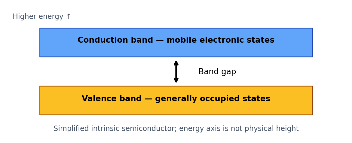
Original educational illustration (schematic; not to scale).
At zero kelvin, a typical intrinsic semiconductor has a filled valence band and an empty conduction band, separated by a band gap. At higher temperatures or under illumination, some electrons can gain enough energy to occupy conduction-band states. The vacancies they leave in the valence band behave as positive charge carriers called holes.
Electrical conduction in semiconductors can involve both conduction-band electrons and holes moving in response to an applied field. That is why the valence band is more than a passive store of electrons: its missing electrons matter to electrical behavior.
What the band gap tells you
The band gap is the minimum relevant energy difference between occupied valence states and accessible conduction states in a simplified band model. The size and character of that gap influence which photons a material absorbs or emits, and how easily carriers can be generated. Silicon, for example, is widely used because its electronic properties are useful for controlling current and making devices.
Energy gaps are often reported in electronvolts (eV). A band gap is not the same as a mechanical gap or thickness of material. Its relationship to absorption can also depend on whether the transition between bands is direct or indirect, so the same energy diagram does not explain every optical feature.
Metals, semiconductors, and insulators
In a metal, available electronic states typically permit conduction without requiring a sizable band-gap transition, because bands may overlap or be partially filled. In many insulators, the energy needed to create mobile carriers is comparatively large. Semiconductors lie between these extremes, with electrical behavior strongly affected by temperature, light, and deliberate addition of dopants.
These categories are useful for engineering but can be more nuanced in real materials. Defects, impurities, crystal structure, and temperature alter practical conductivity.
A common mistake in simple diagrams
A diagram showing an arrow 'jumping the gap' is an energy transition, not an electron physically leaping across empty space inside the solid. Likewise, a hole is not a free-standing positively charged particle in a vacuum; it is a way to describe an unoccupied valence-band state that behaves as a mobile positive carrier.
How light can create carriers
A photon with sufficient energy can promote an electron into an available conduction-band state, leaving a hole behind. In a photodiode or solar cell, electric fields and device structure help separate or collect charge carriers. This connects a band diagram to a real technology without suggesting that a single diagram predicts the efficiency of every material or device.
Frequently asked questions
Is the valence band always full? It is filled in the ideal low-temperature intrinsic-semiconductor picture; real occupation depends on material and conditions.
What happens when an electron crosses the gap? It enters an accessible conduction state and can leave a hole in the valence band.
Does a large gap usually make conduction easier? No. A larger gap generally makes thermal excitation of carriers more difficult, all else equal.
Explore related science topics
For a closer look at connected concepts, read electric and magnetic fields, and mu-metal shielding.